CBSE Class 12th Physics Chapter 14 - Semiconductor Electronics: Materials, Devices and Simple Circuits Important Questions with Answers
You should focus on solving CBSE Class 12th Physics Chapter 14: Semiconductor Electronics: Materials, Devices and Simple Circuits important questions, especially to help you score high marks. By solving CBSE Class 12th Physics 14 questions, you will be solving exam-oriented questions only.
Never Miss an Exam Update
Prepare thoroughly with the most important questions of CBSE Class 12th Physics Chapter 14 - Semiconductor Electronics: Materials, Devices and Simple Circuits. You can first cover the CBSE Class 12th Physics syllabus to understand the key topics and then start solving the CBSE Class 12th Physics Chapter 14 - Semiconductor Electronics: Materials, Devices and Simple Circuits Important Question to get a better understanding of your preparation level. Start practicing now.
It is required to design a (two-input) logic gate, using an appropriate number, of :
(a) NAND gates that gives a ‘low’ output only when both the inputs are ‘low’.
(b) NOR gates that gives a ‘high’ output only when both the inputs are ‘high’.
Draw the logic circuits for these two cases and write the truth table, corresponding to each of the two designs. (Comptt. All India 2017)
Question 2.
For a CE-transistor amplifier, the audio signal voltage across the collector resistance of 2 k? is 2V. Given the current amplification factor of the transistor is 100, find the input signal voltage and base current, if the base resistance is 1 k? (Delhi 2017)
Question 3.
A zener diode is fabricated by heavily doping both p- and n-sides of the junction. Explain, why? Briefly explain the use of zener diode as a dc voltage regulator with the help of a circuit diagram. ‘ (Delhi 2017)
Question 4.
Explain briefly with the help of necessary diagrams, the forward and the reverse biasing of a p-n junction diode. Also draw their characteristic curves in the two cases. (Delhi 2017)
Question 5.
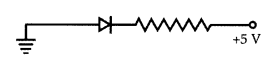
(a) In the given diagram, is the junction diode forward biased or reverse biased?
(b) Draw the circuit diagram of a full wave rectifier and state how it work. (All India 2017)
Question 6.
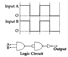
(a) Write the functions of the three segments of a transistor.
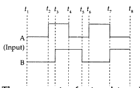
(b) The figure shows the input waveforms A and B for ‘AND’ gate. Draw the output waveform and write the truth table for this logic gate. (All India 2017)
Question 7.
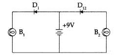
(a) In the given diagram, which bulb out of B1 and B2 will glow and why ?
(b) Draw the circuit diagram of a full wave rectifier and state how it works.
(c) Explain briefly the three processes due to which generation of emf takes place in a solar cell. (All India 2017)
Question 8.
(a) Draw the circuit diagram for studying the characteristics of a transistor in common emitter configuration. Explain briefly and show how input and output characteristics are drawn.
(b) The figure shows input waveforms A and B to a logic gate. Draw the output waveform for an OR gate. Write the truth table for this logic gate and draw its logic symbol. (All India 2017)
Question 9.
(a) Draw the circuit diagram of an n-p-n transistor amplifier in common emitter configuration.
(b) Derive an expression for voltage gain of the amplifier and hence show that the output voltage is in opposite phase with the input voltage. (All India 2017)
Question 10.
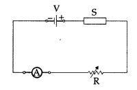
(a) In the given following diagram ‘S’ is a semiconductor. Would you increase or decrease the value of R to keep the reading of the ammeter A constant when S is heated? Give reason for your answer.
(b) The figure shows input waveforms A and B to a logic gate. Draw the output waveform for an OR gate. Write the truth table for this logic gate and draw its logic symbol. (All India 2017)
Great Job! continue working on more practice questions?
Question 1.
Explain the two processes involved in the formulation of a p-n junction diode. Hence define the term ‘barrier potential’. (Comptt. Delhi 2017)
Question 2.
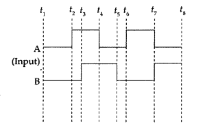
Using the wave forms of the input A and B, draw the output waveform of the given logic circuit. Identify the logic gate obtained. Write also the truth table. (Comptt. Delhi 2017)
Question 3.
State the reason, why the photodiode is always operated under reverse bias. Write the working principle of operation of a photodiode. The semiconducting material used to fabricate a photodiode, has an energy gap of 1.2 eV. Using calculations, show whether it can detect light of wavelength of 400 nm incident on it. (Comptt. All India 2017)
Question 4.
Draw the circuit diagram of a common emitter transistor amplifier. Write the expression for its voltage gain. Explain, how the input and output signals differ in phase by 180°. (Comptt. All India 2017)
Question 5.
Draw the circuit diagram of a full wave rectifier. Explain its working principle. Draw the input and output waveforms. (Comptt. All India 2017)
Question 6.
(a) Explain the formation of depletion layer . and potential barrier in a p-n junction.
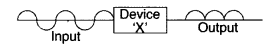
(b) In the figure given below the input waveform is converted into the output waveform by a device ‘X’. Name the device and draw its circuit diagram.
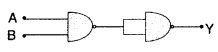
(c) Identify the logic gate represented by the circuit as shown and write its truth table. (Delhi 2017)
Question 7.
(a) With the help of the circuit diagram explain the working principle of a transistor amplifier as an oscillator.
(b) Distinguish between a conductor, a semiconductor and an insulator on the basis of energy band diagrams. (Delhi 2017)
Question 8.
(a) Draw the circuit diagrams of a p-n junction diode in
(i) forward bias,
(ii) reverse bias. How are these circuits used to study the V – I characteristics of a silicon diode? Draw the typical V – I characteristics.
(b) What is a light emitting diode (LED)?
Mention two important advantages of LEDs over conventional lamps. (All India 2017)
Question 9.
(a) Draw the circuit arrangement for studying the input and output characteristics of an n- p-n transistor in CE configuration. With the help of these characteristics define
(i) input resistance,
(ii) current amplification factor.
(b) Describe briefly with the help of a circuit diagram how an n-p-n transistor is used to produce self-sustained oscillations. (All India 2017)
Question 10.
(i) Explain with the help of a diagram the formation of depletion region and barrier potential in a pn junction.
(ii) Draw the circuit diagram of a half wave rectifier and explain its working. (All India 2016)
Great Job! continue working on more practice questions?
Other CBSE Class 12th Physics Chapter Wise Questions